
Synthesis and processing
Chemical Vapour Deposition (CVD) Thin Film and Nanomaterial Synthesis System
Tube-furnace CVD synthesis of graphene, carbon nanotubes, transition metal dichalcogenides and oxide thin films under controlled gas flow and temperature profiles.
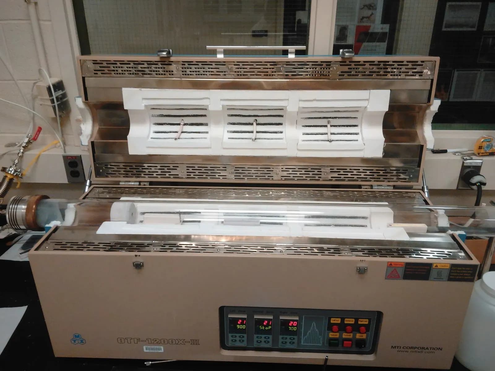
In short
Tube-furnace CVD synthesis of graphene, carbon nanotubes, transition metal dichalcogenides and oxide thin films under controlled gas flow and temperature profiles. The system is a thermal chemical vapour deposition (CVD) platform comprising a quartz reaction tube, a process gas line fed through mass flow controllers (MFC), a vacuum pump and pressure control.
- Process type
- Thermal CVD, tube-furnace configuration
- Reactor
- Quartz reaction tube
- Gas control
- Multi-channel mass flow controllers (Ar, H₂, hydrocarbon and other process gases)
Services on this instrument
Thin Film Deposition: CVD, Spray Pyrolysis and Spin Coating
from €7107–15 business daysRequest this serviceService detailsInstrument Operator Training
from €42014–30 business daysRequest this serviceService details
Overview
The system is a thermal chemical vapour deposition (CVD) platform comprising a quartz reaction tube, a process gas line fed through mass flow controllers (MFC), a vacuum pump and pressure control. Gaseous or vaporised precursors decompose or react at the substrate surface within a controlled temperature zone to form thin films or nanostructures. Typical processes include graphene growth on copper or nickel foil under argon, hydrogen and hydrocarbon flow, carbon nanotube synthesis on catalyst-coated substrates, monolayer growth of transition metal dichalcogenides such as MoS₂ and WS₂, metal oxide and nitride coatings, and atmosphere-controlled annealing. Multi-segment temperature programming, operation from atmospheric to low pressure and programmable gas mixtures allow repeatable growth recipes. The materials produced are characterised in the same centre by Raman, SEM/EDS, XRD and four-point probe measurements.
Measurement principle
Capabilities
Single- and few-layer graphene growth on copper and nickel foil
Carbon nanotube synthesis on catalyst-coated substrates
2D transition metal dichalcogenide films such as MoS₂ and WS₂
Metal oxide and nitride thin film coatings
Atmosphere-controlled annealing in argon, hydrogen and gas mixtures
MFC-controlled, multi-segment repeatable growth recipes
Suitable samples
Copper, nickel and other metal foil substrates
Silicon and SiO₂/Si wafers
Quartz, sapphire and glass substrates
Catalyst-coated supports
Powders and fibrous materials (atmosphere-controlled annealing)
Metal oxide and carbon precursors
Technical specifications
| Process type | Thermal CVD, tube-furnace configuration |
|---|---|
| Reactor | Quartz reaction tube |
| Gas control | Multi-channel mass flow controllers (Ar, H₂, hydrocarbon and other process gases) |
| Pressure range | Atmospheric to low pressure (with vacuum pump) |
| Temperature programming | Multi-segment PID; covers graphene and CNT growth temperatures |
| Typical products | Graphene, CNTs, TMD monolayers, oxide/nitride films |
Services on this instrument
Thin Film Deposition: CVD, Spray Pyrolysis and Spin Coating
from €7107–15 business daysRequest this serviceService detailsInstrument Operator Training
from €42014–30 business daysRequest this serviceService details
- Catalogue no.
- 9
Quick answers
CVD: key facts
What is Chemical Vapour Deposition (CVD) Thin Film and Nanomaterial Synthesis System used for?
It is used for: Single- and few-layer graphene growth on copper and nickel foil, Carbon nanotube synthesis on catalyst-coated substrates, 2D transition metal dichalcogenide films such as MoS₂ and WS₂, Metal oxide and nitride thin film coatings, Atmosphere-controlled annealing in argon, hydrogen and gas mixtures, and MFC-controlled, multi-segment repeatable growth recipes.
Which samples can Chemical Vapour Deposition (CVD) Thin Film and Nanomaterial Synthesis System analyse?
Suitable samples: Copper, nickel and other metal foil substrates, Silicon and SiO₂/Si wafers, Quartz, sapphire and glass substrates, Catalyst-coated supports, Powders and fibrous materials (atmosphere-controlled annealing), and Metal oxide and carbon precursors.
Which NAKTEM services use Chemical Vapour Deposition (CVD) Thin Film and Nanomaterial Synthesis System?
Thin Film Deposition: CVD, Spray Pyrolysis and Spin Coating and Instrument Operator Training.
What results do I receive?
Typical deliverables: Thin film samples deposited on the agreed substrates (labelled, protective packaging), Process record covering precursor/gas composition, temperature, pressure, flow rate, spin speed and duration, Coated area map and visual uniformity assessment, Sheet resistance, thickness, XRD/Raman phase verification or SEM imaging on request, and Process summary report (PDF).
Related services
Sample preparation and processing
Thin Film Deposition: CVD, Spray Pyrolysis and Spin Coating
Functional thin films, oxide coatings and nanomaterial layers produced by chemical vapour deposition, ultrasonic spray pyrolysis and spin coating.
Training
Instrument Operator Training
Hands-on operator training on analytical instruments including SEM/EDS, XRD, Raman and rheometry, covering sample preparation, measurement and data interpretation.
Related instruments
Spectroscopy and diffraction
Olympus BX43F-based Confocal Micro-Raman Spectroscopy System
Laser-excited micro-Raman spectroscopy for chemical and structural identification at micrometre resolution, including phase and defect analysis of carbon materials.
Microscopy and imaging
ZEISS EVO 10 Scanning Electron Microscope with Oxford EDS Detector
Nanometre-scale surface morphology imaging with simultaneous elemental mapping by energy-dispersive X-ray spectroscopy.
Coating and thin film
Siansonic Ultrasonic Spray Pyrolysis Thin-Film Deposition System
Deposition of uniform metal-oxide, conductive and functional thin films on heated substrates by ultrasonic atomisation of precursor solutions.
Electrochemistry and electrical
Ossila P2010A2 Four-Point Probe Sheet Resistance Measurement System
Contact-resistance-independent measurement of sheet resistance, resistivity and conductivity of thin films, coatings and semiconductor wafers.
Request analysis on this instrument
Tell us about your sample and the question. Our scientists confirm feasibility and propose a measurement plan.