Microscopy and imaging
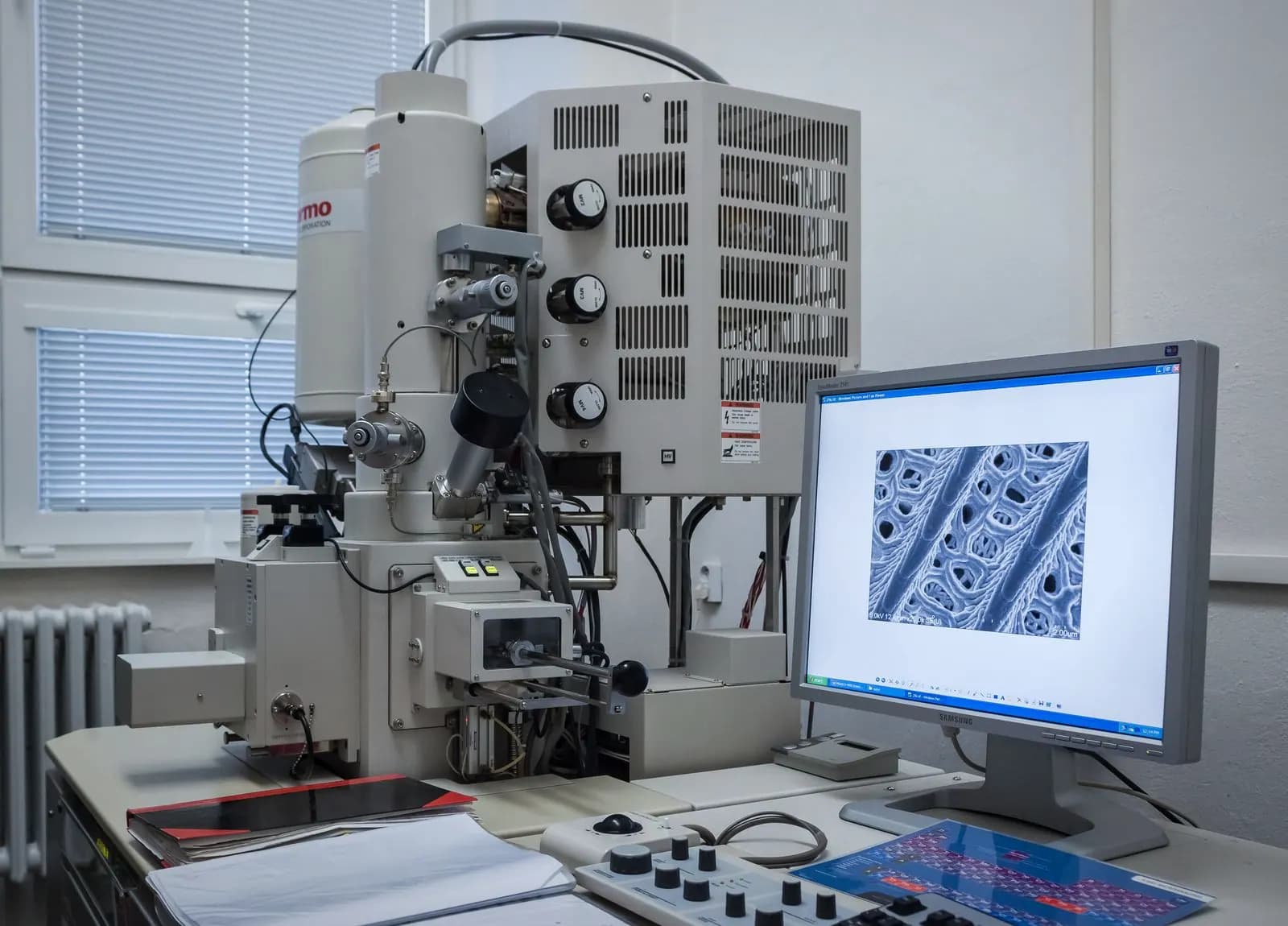
ZEISS EVO 10 Scanning Electron Microscope with Oxford EDS Detector
Nanometre-scale surface morphology imaging with simultaneous elemental mapping by energy-dispersive X-ray spectroscopy.
In short
Nanometre-scale surface morphology imaging with simultaneous elemental mapping by energy-dispersive X-ray spectroscopy. The ZEISS EVO 10 is a versatile tungsten-filament scanning electron microscope operating in both high-vacuum and variable-pressure modes. Non-conductive polymers, ceramics and biological specimens can be examined in variable-pressure mode without conductive coating.
- Electron source
- Tungsten filament
- Accelerating voltage
- 0.2 – 30 kV
- Resolution
- 3 nm @ 30 kV (SE)
Services on this instrument
SEM/EDS Imaging and Microanalysis
from €1703–7 business daysRequest this serviceService detailsFailure Analysis and Materials Consulting
from €7757–14 business daysRequest this serviceService detailsInstrument Operator Training
from €42014–30 business daysRequest this serviceService details
Overview
The ZEISS EVO 10 is a versatile tungsten-filament scanning electron microscope operating in both high-vacuum and variable-pressure modes. Non-conductive polymers, ceramics and biological specimens can be examined in variable-pressure mode without conductive coating. The integrated Oxford Instruments EDS detector complements imaging data with chemical composition through point analysis, line scans and elemental mapping. The system is configured to deliver repeatable, traceable results for quality control, failure analysis and R&D programmes.
Measurement principle
Capabilities
Secondary-electron (SE) and backscattered-electron (BSE) imaging
Variable-pressure mode for uncoated non-conductive specimens
EDS point, line and mapping analysis (elements B to U)
Particle size, porosity and layer thickness measurements
Fracture surface and failure analysis reporting
Suitable samples
Metals and alloys
Ceramics and composites
Polymers and coatings
Powders and nanomaterials
Biological and dried specimens
Technical specifications
| Electron source | Tungsten filament |
|---|---|
| Accelerating voltage | 0.2 – 30 kV |
| Resolution | 3 nm @ 30 kV (SE) |
| Magnification | 5× – 1,000,000× |
| Vacuum modes | High vacuum / variable pressure (10–400 Pa) |
| EDS detector | Oxford Instruments SDD |
Services on this instrument
SEM/EDS Imaging and Microanalysis
from €1703–7 business daysRequest this serviceService detailsFailure Analysis and Materials Consulting
from €7757–14 business daysRequest this serviceService detailsInstrument Operator Training
from €42014–30 business daysRequest this serviceService details
- Manufacturer
- ZEISS
- Model
- EVO 10 + Oxford Instruments EDS
- Catalogue no.
- 19
- Reference standards
- ISO 16700, ASTM E1508, ISO 22309
Quick answers
SEM / EDS: key facts
What is ZEISS EVO 10 Scanning Electron Microscope with Oxford EDS Detector used for?
It is used for: Secondary-electron (SE) and backscattered-electron (BSE) imaging, Variable-pressure mode for uncoated non-conductive specimens, EDS point, line and mapping analysis (elements B to U), Particle size, porosity and layer thickness measurements, and Fracture surface and failure analysis reporting.
Which samples can ZEISS EVO 10 Scanning Electron Microscope with Oxford EDS Detector analyse?
Suitable samples: Metals and alloys, Ceramics and composites, Polymers and coatings, Powders and nanomaterials, and Biological and dried specimens.
Which standards does ZEISS EVO 10 Scanning Electron Microscope with Oxford EDS Detector relate to?
Relevant standards: ISO 16700, ASTM E1508, and ISO 22309.
Which NAKTEM services use ZEISS EVO 10 Scanning Electron Microscope with Oxford EDS Detector?
SEM/EDS Imaging and Microanalysis, Failure Analysis and Materials Consulting, and Instrument Operator Training.
What results do I receive?
Typical deliverables: SE/BSE micrographs with scale bars and acquisition parameters (TIFF/PNG), EDS spectra and point/area analysis tables (weight % and atomic %), Elemental maps and line-scan profiles, Technical report (PDF) covering sample preparation, coating and measurement conditions, and Particle size, thickness or porosity measurement tables on request.
Related services
Analysis
SEM/EDS Imaging and Microanalysis
High-resolution surface imaging by scanning electron microscopy with elemental point, line and map analysis by energy-dispersive X-ray spectroscopy.
Consulting
Failure Analysis and Materials Consulting
Root-cause determination of fracture, corrosion, coating delamination and product performance problems by multi-technique characterisation and expert review.
Training
Instrument Operator Training
Hands-on operator training on analytical instruments including SEM/EDS, XRD, Raman and rheometry, covering sample preparation, measurement and data interpretation.
Related instruments
Coating and thin film
Quorum MiniQS Sputter Coater
Nanometre-thin gold, gold-palladium or platinum conductive coating of non-conductive specimens ahead of SEM imaging and thin-film studies.
Spectroscopy and diffraction
Anton Paar XRDynamic 500 X-ray Diffractometer (XRD)
Crystalline phase identification, quantitative phase analysis, crystallite size and non-ambient structural studies on powders and solid materials.
Spectroscopy and diffraction
Olympus BX43F-based Confocal Micro-Raman Spectroscopy System
Laser-excited micro-Raman spectroscopy for chemical and structural identification at micrometre resolution, including phase and defect analysis of carbon materials.
Further reading
Training
Why Materials Characterization Training Pays Off
A badly prepared sample, a wrongly chosen parameter or an over-interpreted spectrum can cost far more than the instrument itself. We explain why structured characterization training delivers a tangible return for R&D and quality teams.
October 27, 20264 min readCharacterization
SEM/EDS Sample Preparation Guide
Reliable scanning electron microscopy and EDS results begin long before the sample enters the chamber. A hands-on guide to mounting, conductive coating, surface preparation and the mistakes that most often ruin an analysis.
September 22, 20265 min readCharacterization
How to Choose a Particle Size Analysis Method
A practical guide to choosing between laser diffraction, electron microscopy, dynamic light scattering and sieving, based on your sample, your size range and how the result will be used.
September 8, 20265 min read
Request analysis on this instrument
Tell us about your sample and the question. Our scientists confirm feasibility and propose a measurement plan.