
Coating and thin film
Quorum MiniQS Sputter Coater
Nanometre-thin gold, gold-palladium or platinum conductive coating of non-conductive specimens ahead of SEM imaging and thin-film studies.
In short
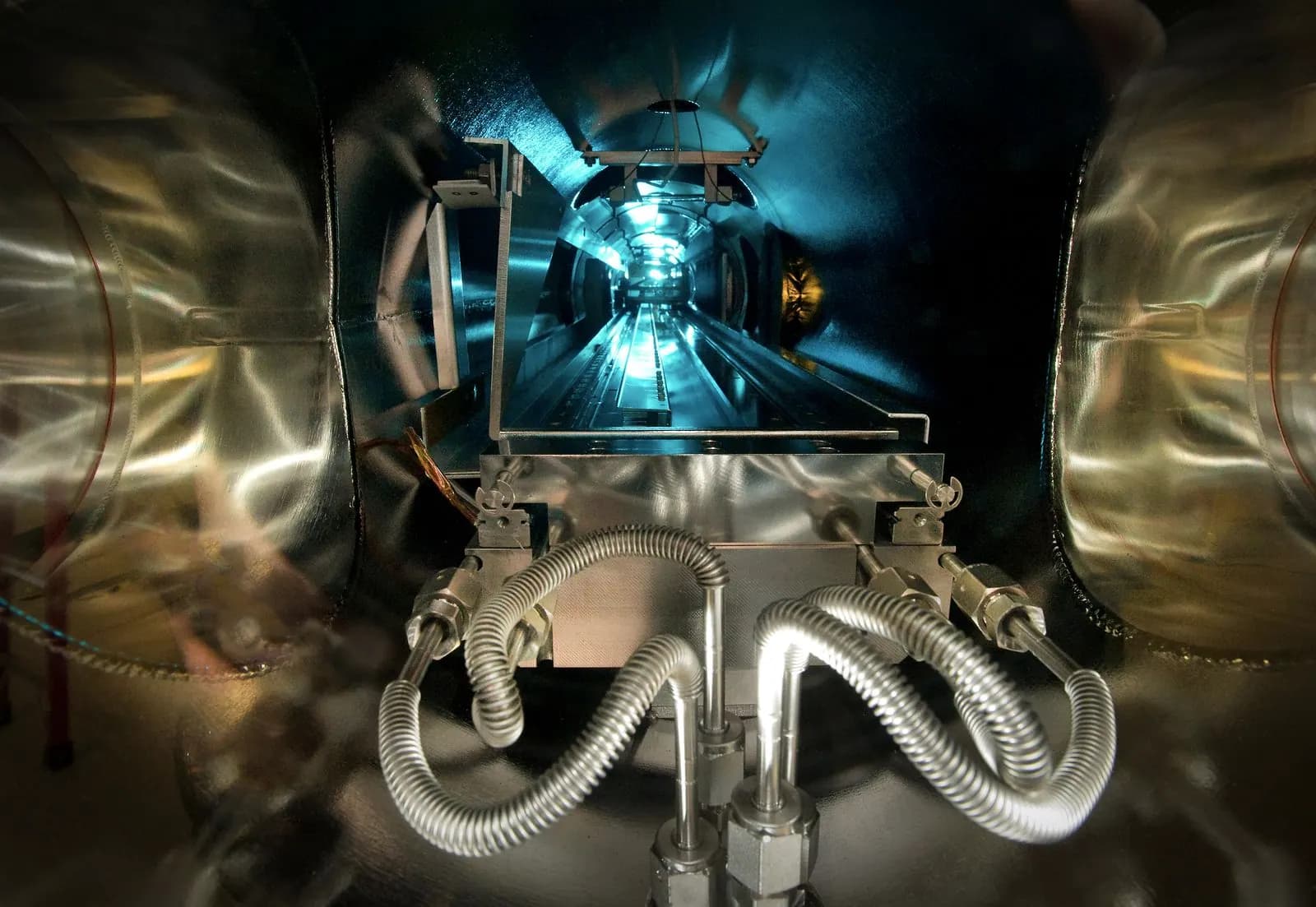
Nanometre-thin gold, gold-palladium or platinum conductive coating of non-conductive specimens ahead of SEM imaging and thin-film studies. The Quorum MiniQS is a compact sputter coater in which metal atoms ejected from a magnetron target in a low-pressure argon plasma form a thin, continuous film on the specimen surface.
- Coating principle
- DC magnetron sputtering
- Target materials
- Au, Au/Pd, Pt
- Process gas
- Argon
Services on this instrument
SEM/EDS Imaging and Microanalysis
from €1703–7 business daysRequest this serviceService detailsInstrument Operator Training
from €42014–30 business daysRequest this serviceService details
Overview
The Quorum MiniQS is a compact sputter coater in which metal atoms ejected from a magnetron target in a low-pressure argon plasma form a thin, continuous film on the specimen surface. With gold, gold-palladium and platinum targets, polymer, ceramic, biological and powder samples are rendered conductive before scanning electron microscopy (SEM), eliminating charging, improving secondary-electron yield and preserving image quality at high magnification. Film thickness is controlled through sputter current and time, and a rotating stage gives even coverage on complex geometries. Beyond SEM sample preparation, the coater is used in thin-film research to deposit metal electrode layers, to create conductive contacts for four-point-probe measurements and to study the relationship between coating thickness and sheet resistance. Its small footprint and short pump-down time support high sample throughput in a microscopy laboratory.
Measurement principle
Capabilities
Conductive coating with Au, Au/Pd and Pt targets
Nanometre-scale film thickness set by current and time
Even coverage of complex surfaces on a rotating stage
Charge-free specimen preparation ahead of SEM
Metal electrode deposition for thin-film and electrical measurements
Short cycle time with rapid pump-down
Suitable samples
Polymer and composite SEM specimens
Ceramic and glass surfaces
Biological and dried tissues
Powder and nanomaterial samples
Silicon and glass substrates
Paper, textiles and membranes
Technical specifications
| Coating principle | DC magnetron sputtering |
|---|---|
| Target materials | Au, Au/Pd, Pt |
| Process gas | Argon |
| Thickness control | Sputter current and time |
| Typical film thickness | A few nanometres to tens of nanometres |
| Specimen stage | Rotating, holds multiple SEM stubs |
Services on this instrument
SEM/EDS Imaging and Microanalysis
from €1703–7 business daysRequest this serviceService detailsInstrument Operator Training
from €42014–30 business daysRequest this serviceService details
- Manufacturer
- Quorum
- Model
- MiniQS
- Catalogue no.
- 20
Quick answers
Sputter Coater: key facts
What is Quorum MiniQS Sputter Coater used for?
It is used for: Conductive coating with Au, Au/Pd and Pt targets, Nanometre-scale film thickness set by current and time, Even coverage of complex surfaces on a rotating stage, Charge-free specimen preparation ahead of SEM, Metal electrode deposition for thin-film and electrical measurements, and Short cycle time with rapid pump-down.
Which samples can Quorum MiniQS Sputter Coater analyse?
Suitable samples: Polymer and composite SEM specimens, Ceramic and glass surfaces, Biological and dried tissues, Powder and nanomaterial samples, Silicon and glass substrates, and Paper, textiles and membranes.
Which NAKTEM services use Quorum MiniQS Sputter Coater?
SEM/EDS Imaging and Microanalysis and Instrument Operator Training.
What results do I receive?
Typical deliverables: SE/BSE micrographs with scale bars and acquisition parameters (TIFF/PNG), EDS spectra and point/area analysis tables (weight % and atomic %), Elemental maps and line-scan profiles, Technical report (PDF) covering sample preparation, coating and measurement conditions, and Particle size, thickness or porosity measurement tables on request.
Related services
Analysis
SEM/EDS Imaging and Microanalysis
High-resolution surface imaging by scanning electron microscopy with elemental point, line and map analysis by energy-dispersive X-ray spectroscopy.
Training
Instrument Operator Training
Hands-on operator training on analytical instruments including SEM/EDS, XRD, Raman and rheometry, covering sample preparation, measurement and data interpretation.
Related instruments
Microscopy and imaging
ZEISS EVO 10 Scanning Electron Microscope with Oxford EDS Detector
Nanometre-scale surface morphology imaging with simultaneous elemental mapping by energy-dispersive X-ray spectroscopy.
Electrochemistry and electrical
Ossila P2010A2 Four-Point Probe Sheet Resistance Measurement System
Contact-resistance-independent measurement of sheet resistance, resistivity and conductivity of thin films, coatings and semiconductor wafers.
Coating and thin film
Laurell WS-650Mz-23NPPB Programmable Spin Coater
Solution-based deposition of uniform polymer, sol-gel and nanomaterial thin films on flat substrates with controlled thickness by spin coating.
Coating and thin film
DeFelsko PosiTector 6000 Coating Thickness Gauge
Non-destructive measurement of paint, plating and thin-film thickness on metal substrates by magnetic induction and eddy-current principles.
Further reading
Characterization
SEM/EDS Sample Preparation Guide
Reliable scanning electron microscopy and EDS results begin long before the sample enters the chamber. A hands-on guide to mounting, conductive coating, surface preparation and the mistakes that most often ruin an analysis.
September 22, 20265 min read
Request analysis on this instrument
Tell us about your sample and the question. Our scientists confirm feasibility and propose a measurement plan.